
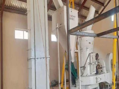
palwriser for pcb process
Dr. Schenk GmbH: Plastic Inspection
Dr. Schenk offers ultrafast, precise and reliable optical plastic inspection and measuring solutions for all kinds of base and converted plastic materials.. EasyInspect examines 100% of the material surface for local defects and EasyMeasure continuously monitors overall properties, such as coating uniformity or homogeneity and physical properties, such as opacity or reflectance.
Partner MASS GmbH pcb in Process
Germany, Austria, Switzerland. Systronic Produktionstechnologie GmbH Co. KG Daimlerstraße 1 74389 Cleebronn Tel.: +49 7135 Fax: +49 7135
Crossed Roller Bearing Picomotor Linear Translation Stages
We've incorporated our Picomotor™ actuators with our crossedrollerbearing translation stages to meet your demanding photonics applications. Crossedrollerbearing motorized stages provide smooth and accurate positioning for critical optical alignment applications such as fiber alignment and highstability positioning in laser systems.
How a screen is manufactured assembled FlatpanelsHD
Jun 30, 2010· Assembly. The next worker prepares the front bezel and adds cushioning material before placing the LCD panel inside. Once the LCD panel is encased inside the bezel, the power PCB and main PCB, manufactured by Eizo at a separate factory, are added. The next part of the assembly process is automated screw insertion.
PCB Manufacturing Process Find Out How PCBs are Made ...
Jul 03, 2018· The PCB connects all of the other components inside, so you can use your electronic device for what it is intended to do. Although they are small, the manufacturing process of a PCB is quite extensive. Whether you are making one yourself or going through a PCB manufacturer, multiple steps are crucial to the development of the board. Because ...
Materials SMT, PCB Manufacturing Products and Services
Durostone sheet for wave solder pallet. Durostone is a fiberreinforced plastic for mechanical and electrical applications. With good performance against electric arc and tracking, it is an ideal material for solder paste printing, SMT process, reflow soldering and wave soldering....
What is the Difference B/W TCB(Thread control block) PCB ...
Feb 29, 2012· 'A process control block (PCB) and a Thread Control Block (TCB) are both used in kernels to have time on the CPU delegated to them' not normally, no. A PCB will have one or more TCB's linked to it. The TCB describes an execution context, (eg. stack pointer), the PCB an environment context, (eg. memory segments and permissions).
Process Control Block PCB Process State Memory Base and ...
Process Control Block (PCB) Typical information contained in a PCB associated with a process Process state – new, ready, running, waiting, halting, . Program counter – Address for next instruction to be executed CPU registers – accumulators, index registers, stack pointers and other general registers CPU scheduling information – process priority, pointers to scheduling queues, and ...
PCB Process PCB Capabilities Why Us PCBA Store
PCB Manufacturing Process — A StepbyStep Guide. At PCBAStore we handle the PCB manufacturing process for customers from start to finish, but we believe it's important that our customers understand what we do this ensures that your design specifications better serve your interests.
PCB inspection / repair Qscope
PCB inspection / repair. INDUSTRY PCB (Printed Circuit Board) and microelectronics manufacturing are critical and therefore demand an imaging solution to accurate build, assemble, inspect, measure and document each part in the manufacturing process.
DEVELOPMENT OF A ONE STEP DECONTAMINATION .
containing PCB contamination would require a two step process whereby radioactivity and heavy metals would be removed in the first step and PCB would be destroyed in the second step. A major disadvantage of this scheme is that a significant degree of oil oxidation takes place in the first step

which surface finish for PCB PCB prototype
which surface finish for PCB. Please find here under a list of PCB surface finish. OSP (Organic Solderability Preservative) or Entek or passivation is an organic finish that bond with is probably the most ecofriendly surface finish, it requires little energy and no toxic materials are used.

PCB Design Layout Guidelines Hints Tips | Electronics ...
Printed circuit board, PCB design, is one of the most important design elements within the design of an electronics product. In most instances an electronics hardware design engineer will design the circuit, and then a PCB layout specialist will undertake the PCB layout and design from a schematic provided using a PCB CAD system.
KK Interconnection System Molex | Mouser
Molex KK Interconnection System consists of connectors that form the building block for creating thousands of different configurations. This connector system offers many polarization features that ensure correct mating. The KK interconnection systems incorporate offset header entry holes that ...
PCB Etching Process Steps HowTo Video
PCB etching process is one of the major steps in the chemical processing of subtractive printed circuit board. It is the removal of copper, to achieve the desired circuit patterns. In PCB etching process, all copper is removed except the circuitry that is protected by the tin plating applied during the previous treatment in PCB manufacture.
PCB Prototype PCB Fabrication Manufacturer JLCPCB
JLCPCB(Shenzhen JLC Electronics Co., Ltd.), is the largest PCB prototype enterprise in China and a hightech manufacturer specializing in quick PCB prototype and smallbatch PCB production. With Over 10 years of PCB manufacturing experience, we're able to provide cost effective solutions that deliver the highest reliability PCB products to ...
How To Get Satisfied PCB Silkscreen A StepbyStep Guide
PCB silkscreen is a subprocess in the board tree of solder masking along with other ones as baking, UV exposure and developing. However, due to its overall impact on the product's grading and its reliability, you can consider it as the most sophisticated ones among the four in its class.
A flow chart to understand PCB designing process
PCB design flow chart explains various steps involved in the process of PCB designing.
Effect of Machine Parameters on Drilling Process of PCB
What is Printed Circuit Board (PCB)? A PCB is a thin board made of fiberglass, composite epoxy, or other laminate material. Conductive pathways are etched or "printed" onto board, connecting different components on the PCB, such as transistors, resistors, and integrated circuits. PCBs are used in both desktop and laptop computers.
Etchback PCB Co
Printed Circuit Board Etchback. NEGATIVE ETCHBACK Typically when a PCB is manufactured, Plated Though Holes (PTH) are manufactured through a process which begins with the laminate material containing the copper conduction land being drilled. After a number of intermediate processes, the drilled holes which are to be plated are cleaned (or ...

Innovative High Throw Copper Electrolytic Process
for the PCB manufactures. High throwing power electrolytes are becoming increasingly important, due to the electronic industry requirements of manufacturing high aspect ratio circuit boards. It is shown in this paper that utilizing an innovative DC copper plating system a reliable copper metallization of high aspect ratio PCB can be achieved.
New PCB Plating Process Is Reshoring Success for Whelen ...
1/17/2018 New PCB Plating Process Is Reshoring Success for Whelen Engineering : Products Finishing ... The tact requirement to achieve 100 percent reshoring was PC board output of 50 panels per hour; translating to 2,500 per week of 18 by 24inch and 21 by 24inch rigid and
LCD COF/TAB Bonding Process Steps | LCD TV Repair Machine
Mar 03, 2019· 2. Glass and side PCB fixation Usage: Make a fixation between Glass and Side PCB, this can prevent other COFs from damage during bonding process. 3. Polarizer protection Usage: The polarizer may get scratched during bonding process. Put a film (Like preservative film) on the polarizer can solve this problem.
Optical Materials for Lamp, Light Modules and Luminaires
SiliconBased Technologies to Enhance LED Lighting Bring More Light to Any Design. Moldable optical silicones deliver a high level of design freedom in challenging applications such as automotive, general, professional and consumer lighting and outdoor displays. Benefits include: Longterm performance of lighting designs beyond the capability of traditional optical materials like PC and PMMA.